- 您现在的位置:买卖IC网 > Sheet目录317 > C8051F930-TB (Silicon Laboratories Inc)BOARD TARGET/PROTO W/C8051F930
�� �
�
�C8051F93x/92x�
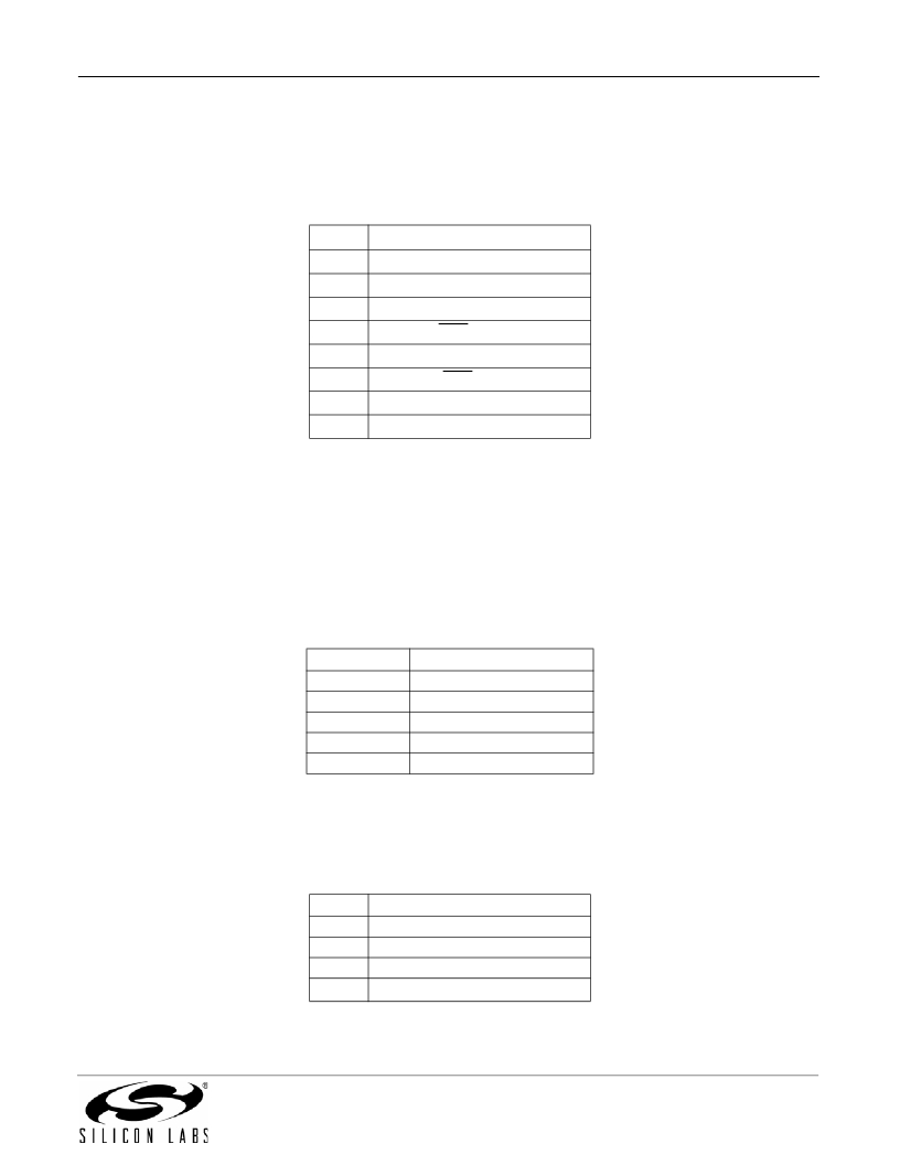
�5.7.� Target� Board� DEBUG� Interface� (J9)�
�The� DEBUG� connector� J9� provides� access� to� the� DEBUG� (C2)� pins� of� the� C8051F930.� It� is� used� to� connect� the�
�Serial� Adapter� or� the� USB� Debug� Adapter� to� the� target� board� for� in-circuit� debugging� and� Flash� programming.�
��Table� 3.� DEBUG� Connector� Pin� Descriptions�
�Pin� #�
�1�
�2,� 3,� 9�
�4�
�5�
�6�
�7�
�8�
�10�
�Description�
�+3� VD� (+3.3� VDC)�
�GND� (Ground)�
�P2.7/C2D�
�RST� (Reset)�
�P2.7�
�RST/C2CK�
�Not� Connected�
�USB� Power� (+5� VDC� from� J9)�
�5.8.� Serial� Interface� (J12)�
�A� USB-to-UART� bridge� circuit� (U3)� and� USB� connector� (P3)� are� provided� on� the� target� board� to� facilitate� serial�
�connections� to� UART0� of� the� C8051F930.� The� Silicon� Labs� CP2103� (U3)� USB-to-UART� bridge� provides� data�
�connectivity� between� the� C8051F930� and� the� PC� via� a� USB� port.� The� VIO� power� supply� and� TX,� RX,� RTS� and�
�CTS� signals� of� UART0� may� be� connected� to� the� CP2103� by� installing� shorting� blocks� on� header� J12.� The� shorting�
�block� positions� for� connecting� each� of� these� signals� to� the� CP2103� are� listed� in� Table� 4.� To� use� this� interface,� the�
�USB-to-UART� device� drivers� should� be� installed� as� described� in� Section� 4.4.� "CP210x� USB� to� UART� VCP� Driver�
��Table� 4.� Serial� Interface� Header� (J12)� Description�
�Header Pins UART0 Pin Description�
�J12[9–10]�
�J12[7–8]�
�J12[5–6]�
�J12[3–4]�
�J12[1–2]�
�CP2103_VIO� (VDD/DC+)�
�TX_MCU� (P0.5)�
�RX_MCU� (P0.4)�
�RTS� (P0.6)�
�CTS� (P0.7)�
�5.9.� Analog� I/O� (H1)�
�Several� of� the� C8051F930� target� device’s� port� pins� are� connected� to� the� H1� terminal� block.� Refer� to� Table� 5� for� the�
�H1� terminal� block� connections.�
�Table� 5.� H1� Terminal� Block� Pin� Descriptions�
�Pin� #�
�1�
�2�
�3�
�4�
�Description�
�P0.6/CNVSTR�
�P0.7/IREF0�
�GND� (Ground)�
�P0.0/V� REF� (Voltage� Reference)�
�Rev.� 0.6�
�17�
�发布紧急采购,3分钟左右您将得到回复。
相关PDF资料
C8051T610DB24
DAUGHTER BOARD T610 24QFN SOCKET
C8051T630DB20
BOARD SOCKET DAUGHTER 20-QFN
CAN-100
BOARD EVAL RS232 100QFP
CANADAPT28
KIT ADAPTER CANDEMOBOARD 28PLCC
CAT24AA01WI-GT3
IC EEPROM SERIAL 1KB I2C 8SOIC
CAT24AA02WI-G
IC EEPROM SERIAL 2KB I2C 8SOIC
CAT24C01ZI-G
IC EEPROM SERIAL 1KB I2C 8MSOP
CAT24C03WI-G
IC EEPROM SERIAL 2KB I2C 8SOIC
相关代理商/技术参数
C8051F931
制造商:SILABS 制造商全称:SILABS 功能描述:25 MIPS, 8 kB Flash, Ultra Low Power, Capacitive Sensing MCU
C8051F931-F-GM
制造商:Silicon Laboratories Inc 功能描述:64KB,10ADC,24PIN MCU (LEAD FREE) - Rail/Tube 制造商:Silicon Laboratories Inc 功能描述:MCU 64KB FLASH 10BIT ADC 24QFN
C8051F931-F-GMR
制造商:Silicon Laboratories Inc 功能描述:64KB,10ADC,24PIN MCU - Tape and Reel 制造商:Silicon Laboratories Inc 功能描述:IC MCU 64KB FLASH 24QFN
C8051F931-G-GM
制造商:Silicon Laboratories Inc 功能描述:64KB/4KB RAM, 10B ADC, DC-DC, 0.9V, QFN24 - Rail/Tube 制造商:Silicon Laboratories Inc 功能描述:IC MCU 8BIT 64KB FLASH 24QFN
C8051F931-G-GMR
制造商:Silicon Laboratories Inc 功能描述:64KB/4KB RAM, 10B ADC, DC-DC, 0.9V, QFN24 - Tape and Reel 制造商:Silicon Laboratories Inc 功能描述:IC MCU 8BIT 64KB FLASH 24QFN
C8051F931-GM
功能描述:8位微控制器 -MCU 64KB 10ADC MCU LEAD FREE
RoHS:否 制造商:Silicon Labs 核心:8051 处理器系列:C8051F39x 数据总线宽度:8 bit 最大时钟频率:50 MHz 程序存储器大小:16 KB 数据 RAM 大小:1 KB 片上 ADC:Yes 工作电源电压:1.8 V to 3.6 V 工作温度范围:- 40 C to + 105 C 封装 / 箱体:QFN-20 安装风格:SMD/SMT
C8051F931-GMR
功能描述:8位微控制器 -MCU 64KB 10ADC MCU LEAD FREE
RoHS:否 制造商:Silicon Labs 核心:8051 处理器系列:C8051F39x 数据总线宽度:8 bit 最大时钟频率:50 MHz 程序存储器大小:16 KB 数据 RAM 大小:1 KB 片上 ADC:Yes 工作电源电压:1.8 V to 3.6 V 工作温度范围:- 40 C to + 105 C 封装 / 箱体:QFN-20 安装风格:SMD/SMT
C8051F93X
制造商:未知厂家 制造商全称:未知厂家 功能描述:Single/Dual Battery, 0.9–3.6 V, 64/32 kB, smaRTClock, 10-Bit ADC MCU